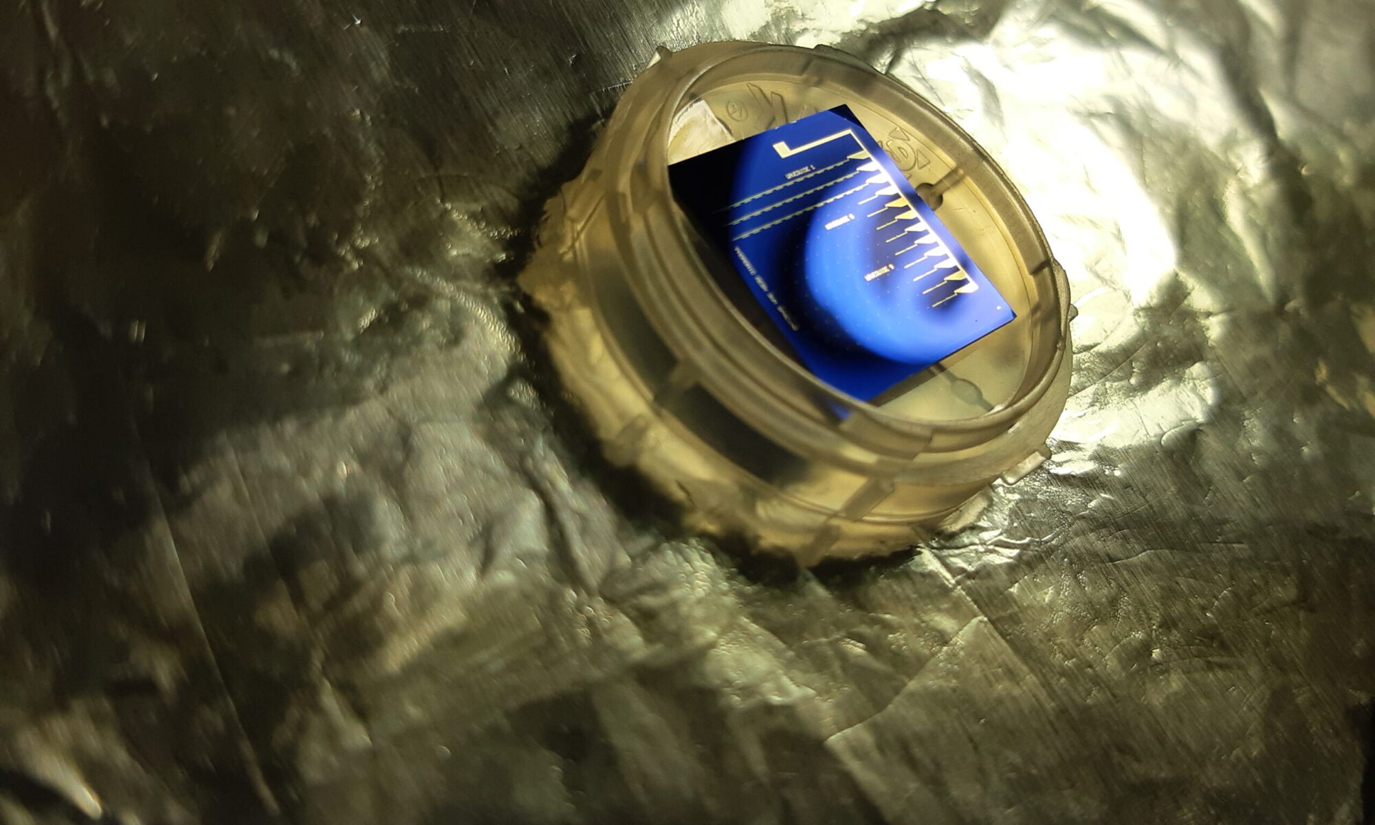
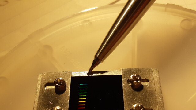
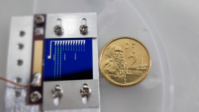
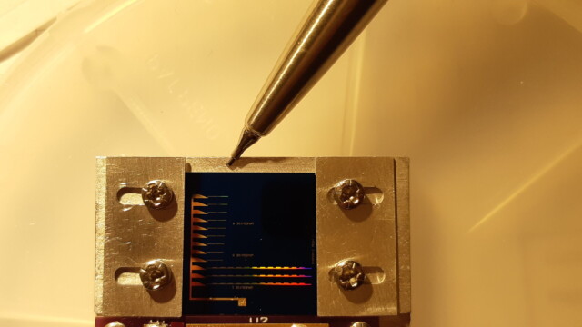
The goal of this research is to develop the building blocks for scalable integrated phononic circuits, similar to those existing in the electronic and optical realms. Phononic circuits have many potential applications, including scalable computing based on mechanical vibrations, or phonons, confined at nanoscale in acoustic waveguides on a silicon chip. Nanomechanical computers of this kind promise inherent robustness to the ionising radiation that degrades semiconductor electronics in low-earth-orbit and deep space environments, as well as in close proximity to nuclear reactors and particle accelerators.
Recent work:
- Propagation and Imaging of Mechanical Waves in a Highly Stressed Single-Mode Acoustic Waveguide, Physical Review Applied, 11, 6, 2019. (Read more below)
- Tunneling of Transverse Acoustic Waves on a Silicon Chip, Phys. Rev. Applied 15, 054036, 2021. (Read more below)
Propagation and Imaging of mechanical waves in a highly stressed single-mode acoustic waveguide


We developed a single-mode acoustic waveguide that enables robust propagation of mechanical waves. The waveguide is a highly stressed silicon-nitride membrane that supports the propagation of out of-plane modes. In direct analogy to rectangular microwave waveguides, there exists a band of frequencies over which only the fundamental mode is allowed to propagate, while multiple modes are supported at higher frequencies. We directly image the mode profiles using optical heterodyne vibration measurement, showing good agreement with theory. In the single-mode frequency band, we show low-loss propagation (approximately 1 dB/cm) for an approximately 5-MHz mechanical wave. This design is well suited for acoustic circuits interconnecting elements such as nonlinear resonators or optomechanical devices for signal processing, sensing, or quantum technologies.
Read more:
- “Propagation and Imaging of Mechanical Waves in a Highly Stressed Single-Mode Acoustic Waveguide,” Physical Review Applied, 11, 6, 2019.
Imaging of acoustic wave tunnelling and exponential decay

Nanomechanical circuits for transverse acoustic waves promise to enable new approaches to computing, precision biochemical sensing and many other applications. However, progress is hampered by the lack of precise control of the coupling between nanomechanical elements. Here, we demonstrate virtual-phonon coupling between transverse mechanical elements, exploiting tunnelling through a zero-mode acoustic barrier. This allows the construction of large-scale nanomechanical circuits on a silicon chip, for which we develop a new scalable fabrication technique. As example applications, we build mode-selective acoustic mirrors with controllable reflectivity and demonstrate acoustic spatial mode filtering. Our work paves the way towards applications such as fully nanomechanical computer processors and distributed nanomechanical sensors, and to explore the rich landscape of nonlinear nanomechanical dynamics.
Read more:
- Mauranyapin, N. P. et al. Tunnelling of transverse acoustic waves on a silicon chip. arXiv:2103.13008 [cond-mat, physics:physics] (2021).
Links:
- PhD Thesis by Erick Romero
https://espace.library.uq.edu.au/view/UQ:e573194
We gratefully acknowledge funding from:


